





Transceiver operation works through electrical conversion
 Nov 04, 2025|
Transceiver operation fundamentally relies on electrical conversion-transforming electrical signals into transmittable forms like optical or radio frequency, then converting received signals back to electrical format. This dual conversion process enables bidirectional data exchange across fiber optic networks, wireless systems, and Ethernet connections by transforming energy between the electrical domain your devices understand and the physical medium optimized for transmission.
Understanding transceiver operation requires examining two discrete stages: a transmit path that encodes outgoing electrical data onto light or RF carriers, and a receive path that decodes incoming signals back into electrical impulses your network equipment can process.
The Electrical-to-Optical Conversion Path
Transceiver operation during transmission involves a coordinated sequence of electrical transformations before converting to optical energy.
The process begins with signal conditioning. Incoming electrical signals from your network device-typically differential pairs carrying high-speed digital data-pass through pre-amplifier circuits that normalize voltage levels and clean up signal edges. This step ensures the data maintains integrity before more aggressive processing.
Next, a laser driver circuit takes over. This specialized component modulates current through a laser diode based on the input data pattern. Modern transceivers perform this operation at speeds exceeding 100 billion times per second for 100 Gbps links. The precision required is extraordinary: timing errors of even 25 picoseconds can corrupt data.
The laser diode itself performs the actual electrical-to-optical conversion. When electrical current passes through the semiconductor junction, electrons recombine with holes and release energy as photons. For multimode fiber systems, vertical-cavity surface-emitting lasers (VCSELs) operating at 850 nm generate this light. Single-mode long-distance systems use distributed feedback (DFB) lasers at 1310 nm or 1550 nm wavelengths for reduced signal dispersion.
The light intensity directly corresponds to the binary data: high optical power represents a "1" bit, low power represents "0." Advanced systems use four-level pulse amplitude modulation (PAM4), where each light pulse encodes two bits through four distinct power levels, effectively doubling data rates without increasing transmission frequency.
Modern transceivers achieve remarkable efficiency in this conversion. Laser-to-fiber coupling efficiencies now exceed 80%, meaning most generated photons successfully enter the fiber core rather than scattering as heat. This efficiency becomes critical at 400 Gbps and beyond, where power budgets directly impact data center operational costs.
The Optical-to-Electrical Receive Process
The receive path reverses this conversion, transforming incoming light pulses back into electrical signals through photodetection.
Light entering from the fiber strikes a photodiode-either a PIN (positive-intrinsic-negative) photodiode or an avalanche photodiode (APD) depending on sensitivity requirements. These semiconductor devices exploit the photovoltaic effect: incoming photons excite electrons across the bandgap, generating electrical current proportional to light intensity.
PIN photodiodes convert light directly into current and work well for short to medium distances where received optical power remains relatively strong. APDs include an internal gain mechanism that amplifies the photocurrent through avalanche multiplication, making them suitable for long-distance links where signals arrive significantly weakened.
The generated photocurrent is extremely weak-often measured in microamperes. A transimpedance amplifier (TIA) converts this tiny current into usable voltage while adding minimal noise. This amplification stage determines the receiver's sensitivity, or its ability to detect weak signals after long fiber runs. Premium 100G transceivers can reliably detect signals as weak as -24 dBm, roughly one-billionth of a watt.
Following amplification, a clock and data recovery (CDR) circuit performs signal reconstruction. The CDR extracts timing information from the received signal pattern and regenerates clean digital output with proper logic levels. This compensates for jitter accumulated during transmission-random timing variations that accumulate as signals traverse hundreds or thousands of meters of fiber.
The recovered electrical signal finally exits the transceiver through differential output pairs, connecting to your switch or router's SerDes (serializer/deserializer) circuits for further processing. The entire receive chain operates in nanoseconds, converting photons back to meaningful electrical data faster than human perception can track.
Modulation and Signal Encoding Methods
Transceiver operation relies heavily on how electrical data gets encoded onto optical carriers, significantly impacting transmission capacity and reach.
On-off keying (OOK) represents the simplest modulation scheme: laser on equals binary 1, laser off equals binary 0. This straightforward approach dominated early optical systems and still appears in short-reach applications. OOK's primary advantage is receiver simplicity-you only need to distinguish between two optical power levels.
However, OOK hits bandwidth limitations as data rates climb. Transmitting 100 Gbps using binary OOK requires switching the laser 100 billion times per second, which challenges laser response times and creates electromagnetic compatibility issues from rapid current changes.
PAM4 modulation addresses this constraint by using four distinct optical power levels instead of two. Each transmitted symbol represents two bits of information. A laser operating at 56 GHz symbol rate can transmit 112 Gbps of data. This approach powers most 400 Gbps transceivers deployed in 2024-2025, with QSFP-DD modules using eight 50 Gbps PAM4 lanes to achieve 400 Gbps aggregate throughput.
The tradeoff with PAM4 involves signal-to-noise ratio requirements. Distinguishing between four power levels demands more precise receivers and cleaner signals compared to binary detection. As a result, PAM4 links show reduced reach compared to OOK at equivalent power levels.
Coherent modulation takes encoding further by manipulating both the amplitude and phase of the optical carrier wave. These systems extract far more information per transmitted symbol-up to 6 bits per Hz of spectrum in advanced implementations. Coherent transceivers enable 400 Gbps transmission over metro and long-haul distances exceeding 80 kilometers, a range impossible with direct-detection methods.
The electrical DSP (digital signal processing) required for coherent transceiver operation represents a significant engineering achievement. Modern coherent transceivers contain ASICs executing trillions of mathematical operations per second to decode the multilevel signals, all while consuming under 15 watts.
Full-Duplex Operation and Channel Separation
Modern transceiver operation predominantly uses full-duplex mode, enabling simultaneous transmission and reception without interference.
The physical implementation typically uses separate channels for each direction. In fiber optic systems, two fiber strands provide the separation: one strand dedicated to transmission, the other to reception. This approach eliminates collision detection complexity and delivers maximum throughput-a 100 Gbps full-duplex link provides 100 Gbps in each direction simultaneously, for 200 Gbps aggregate bandwidth.
Bidirectional (BiDi) transceiver operation achieves full-duplex on a single fiber strand through wavelength-division multiplexing. One direction transmits at 1310 nm while receiving at 1550 nm; the transceiver on the opposite end inverts these wavelengths. Optical filters called wavelength-division multiplexers separate the two signals at each end, preventing transmit light from reaching the local receiver.
This wavelength separation must be carefully managed. A BiDi transceiver designed for 1310 nm TX / 1550 nm RX cannot be paired with another module having the same wavelength assignment. The fiber link requires complementary pairs: if one end transmits 1310 nm, the other must transmit 1550 nm.
RF transceivers in wireless systems achieve full-duplex through frequency-division duplexing (FDD): transmit and receive occur on different frequency bands separated by enough spectrum that filters can isolate them. Alternatively, time-division duplexing (TDD) alternates between transmit and receive time slots on the same frequency, though this technically constitutes high-speed half-duplex rather than true simultaneous operation.
The performance difference between duplex modes is substantial. Full-duplex effectively doubles throughput compared to half-duplex at the same raw data rate. For high-performance computing clusters and data centers, this bidirectional capacity proved critical for east-west traffic patterns where servers exchange data in both directions continuously.
According to market data from 2024, over 95% of newly shipped data center optical transceivers include full-duplex capability as standard, with half-duplex relegated to legacy industrial automation and specialized IoT applications where cost and power consumption outweigh performance requirements.
Form Factors and Electrical Interface Standards
The physical packaging of transceivers evolved alongside data rate requirements, with each generation optimizing electrical and thermal characteristics.
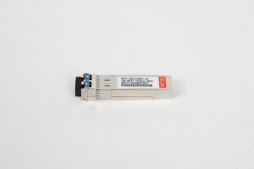
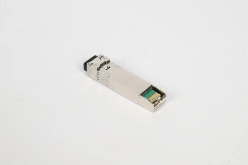
Small form-factor pluggable (SFP) transceivers measure 56mm × 14mm × 9mm and support data rates from 1 Gbps to 10 Gbps. Their compact size enabled 48-port switches in a single rack unit, and hot-swap capability allows field replacement without network downtime. The electrical interface uses differential signaling at 1.25 GHz for gigabit Ethernet or 10.3125 GHz for 10 gigabit links.
Quad small form-factor pluggable (QSFP) modules introduced parallel architecture to reach higher speeds without pushing individual lanes beyond cost-effective frequencies. QSFP28 achieves 100 Gbps by bonding four 25 Gbps electrical lanes, each running at 25.78125 GHz. This parallel approach distributes heat generation and allows graceful degradation-if one lane fails, the link continues operating at 75 Gbps rather than failing completely.
The QSFP28 form factor (72mm × 18.4mm × 8.5mm) became dominant for 100G applications starting in 2016. By 2024, these modules represented 38% of data center transceiver deployments, with annual shipments projected to exceed 15 million units in 2025.
The current frontier involves 400G and 800G transceivers in QSFP-DD (double density) and OSFP form factors. QSFP-DD doubles the lane count to eight while maintaining QSFP mechanical compatibility, achieving 400 Gbps with 50 Gbps lanes or 800 Gbps with 100 Gbps lanes using PAM4 modulation. The electrical interface complexity increases proportionally: maintaining signal integrity across eight 100 GHz differential pairs in a compact module requires sophisticated PCB design and impedance control.
OSFP transceivers measure larger (107mm × 22.6mm × 8.5mm) to accommodate the higher power dissipation of 800G operation-up to 12.5 watts in some modules. This additional thermal headroom proves essential as data rates push beyond what passive cooling can handle in high-density installations.
The electrical pinout standardization through multi-source agreements (MSAs) ensures interoperability. A QSFP28 module from any compliant manufacturer works in any QSFP28-compatible switch port, regardless of vendor. This standardization enabled a robust third-party transceiver market, offering alternatives to OEM modules at 5-10x lower cost for comparable electrical and optical specifications.
Component-Level Architecture
Successful transceiver operation depends on discrete components working in concert to perform the conversions.
The transmit optical subassembly (TOSA) contains the laser diode, monitor photodiode, and coupling optics. The monitor photodiode tracks laser output power, enabling closed-loop control that compensates for temperature variations and aging effects. Modern transceivers maintain optical power within ±1 dB across their operational temperature range of 0-70°C through this feedback mechanism.
The receive optical subassembly (ROSA) houses the photodiode, TIA, and limiting amplifier. Integration of the TIA directly with the photodiode minimizes capacitance and maximizes bandwidth-a critical consideration when detecting 50+ Gbps signals where parasitic capacitance of even a few hundred femtofarads degrades performance.
A microcontroller manages housekeeping functions including digital diagnostic monitoring (DDM). This feature, standardized in SFF-8472 and SFF-8636 specifications, provides real-time readout of transmit power, receive power, temperature, supply voltage, and laser bias current. Network management systems query these parameters to detect failing transceivers before complete failure or to diagnose marginal links.
Power management circuitry converts the host-supplied voltage (typically 3.3V) to the multiple rails required internally: 1.2V for digital logic, 1.8V for analog circuits, and current-controlled supplies for the laser diode. High-efficiency regulators minimize power conversion losses, which contribute directly to module temperature rise.
The electrical interface circuits include input equalizers that compensate for transmission line losses on the host PCB, and output drivers that generate the differential signal levels specified by the electrical standard (typically 400-800 mV differential). Clock and data recovery circuitry reconstructs timing information, ensuring the transceiver can handle jittery input signals from less-than-perfect PCB routing.
Practical Reliability Considerations
Several factors influence transceiver operation reliability in deployed networks.
Optical contamination represents the most common failure mode. A dust particle 10 micrometers in diameter blocking the fiber endface can attenuate 30% of transmitted light in a single-mode system-enough to push received power below detection thresholds. Fiber inspection scopes reveal contamination invisible to the naked eye. Best practice mandates cleaning fiber connectors before every connection, even on new transceivers, using lint-free wipes and >99% isopropyl alcohol or specialized optical cleaning fluid.
Thermal management directly impacts transceiver operation performance and lifespan. Laser diodes show temperature-dependent output power curves: output decreases as junction temperature rises. Most transceivers specify maximum case temperature of 70°C. Exceeding this thermal limit reduces transmit power, potentially degrading link margins to the point of data errors. Data centers must maintain adequate cooling airflow, typically 10-15 cubic feet per minute per module at front panel, to prevent thermal throttling.
Power level matching prevents receiver damage and ensures optimal performance. Long-reach transceivers output +4 to +8 dBm to overcome fiber attenuation over 40-80 kilometers. Short-reach receivers expect -20 to -7 dBm input. Directly connecting high-power transmitters to short-distance receivers can saturate the photodiode, causing bit errors or permanent damage. Optical attenuators (fiber patch cables with calibrated loss) solve this mismatch in scenarios mixing different transceiver types.
Wavelength compatibility checking prevents frustrating "no light" problems. Multimode transceivers at 850 nm require multimode fiber with 50 or 62.5 micrometer core diameter. Single-mode transceivers at 1310 nm or 1550 nm need single-mode fiber with 9 micrometer core. The specifications aren't interchangeable-attempting to use 850 nm transceivers on single-mode fiber results in massive coupling loss and link failure.
BiDi transceivers require particular attention to wavelength pairing. Each end of the link must have complementary TX/RX wavelengths. Checking the transceiver label or DDM information before installation prevents the common mistake of installing matching transceivers that both transmit on the same wavelength.
Mean time between failures for quality transceivers exceeds 500,000 hours-approximately 57 years of continuous operation. Real-world service life typically reaches 7-10 years, more often limited by technology obsolescence than component failure. Laser diodes gradually degrade, losing 0.5-1 dB of output power after 50,000 hours of operation, but generally remain within specification throughout the transceiver's useful lifetime.
Current Market Landscape and Adoption
The global optical transceiver market reached $13.6 billion in 2024, with growth projections climbing toward $25 billion by 2029 driven by data center expansion, 5G infrastructure deployment, and AI training cluster buildouts.
The 100G segment maintained dominance through 2024, accounting for approximately 40% of unit shipments. QSFP28 transceivers power most Top-of-Rack to aggregation layer connectivity in cloud-scale data centers. However, 400G deployment accelerated sharply in 2025, with hyperscale operators transitioning spine layers to 400G QSFP-DD modules to support growing east-west traffic from distributed computing workloads.
The 800G market, practically nonexistent in 2023, approached $2 billion in 2025 as AI infrastructure drove demand for massive inter-GPU bandwidth. These installations use 800G for spine-to-leaf connections, with 1.6 terabit transceivers entering early trials in late 2024 for next-generation clusters.
Geographically, North America represented the largest market in 2024 at approximately 35% of global revenue, driven by hyperscaler data center construction. Asia-Pacific showed the fastest growth rate at 18% CAGR, fueled by 5G network deployment across China, India, and Southeast Asia requiring millions of optical transceivers for backhaul and fronthaul connections.
The compatible transceiver segment-third-party modules coded to work in OEM equipment-expanded to $4.2 billion in 2024, representing roughly 30% of the total market. Organizations seek to reduce networking costs, with compatible transceivers offering identical electrical and optical performance at 80-90% cost savings compared to vendor-branded alternatives. Quality third-party manufacturers achieve >99% compatibility rates through rigorous platform testing and programming appropriate identification EEPROM data.
Frequently Asked Questions
What's the difference between electrical and optical domains in transceiver operation?
The electrical domain refers to voltage and current signals your network equipment produces and understands-typically differential pairs at 0.4-0.8V amplitude. The optical domain uses photons traveling through fiber at specific wavelengths. Transceivers bridge these domains because electrical signals attenuate rapidly over distance (100 meters for copper Ethernet), while optical signals in fiber can travel 100 kilometers with minimal loss.
How does a transceiver prevent its transmitter from interfering with its receiver?
In full-duplex optical transceivers, physical separation solves this: two separate fiber strands keep transmit and receive signals isolated. BiDi transceivers use different wavelengths (1310 nm and 1550 nm) with optical filters separating them. RF transceivers use frequency separation or time-division multiplexing. Without these isolation mechanisms, the strong local transmit signal would completely overwhelm the weak received signal.
Can you mix different transceiver brands on opposite ends of a link?
Yes, provided they share compatible specifications: same data rate, wavelength, fiber type, and connector. Standards ensure interoperability between vendors. I've successfully connected Cisco, Juniper, and third-party transceivers across hundreds of links. The key is matching electrical (10G, 25G, etc.) and optical (wavelength, fiber mode) parameters exactly.
Why do some transceivers require firmware updates while others don't?
Most basic transceivers contain simple microcontrollers with fixed firmware-no update mechanism exists. However, advanced coherent transceivers and some 400G/800G modules include field-updatable firmware to address bugs or enable new modulation schemes. These updates typically install through the host device management interface. Check the datasheet: if firmware updates are mentioned, your equipment likely supports it.
The fundamental principles of transceiver operation remain consistent across types: electrical input drives optical output through laser diodes or generates RF through oscillators, while photodiodes or demodulators convert received signals back to electrical form. This energy domain transformation enables global connectivity, powering everything from video calls to cloud computing infrastructure. As data rates continue climbing toward terabits per second, transceiver operation faces intensifying challenges, requiring ever more sophisticated signal processing, tighter tolerances, and advanced materials to maintain signal integrity across the transitions.