





Transceiver High Bandwidth Handles Data Traffic
 Oct 31, 2025|
A transceiver high bandwidth solution manages data traffic by converting electrical signals to optical signals and transmitting multiple data streams simultaneously over fiber optic cables. These devices use advanced modulation techniques like PAM4 to double data transmission capacity without increasing physical infrastructure, achieving speeds from 100 Gbps to 1.6 Tbps per port.
The global optical transceiver market reached $12.62 billion in 2024 and is projected to hit $42.52 billion by 2032, reflecting annual growth exceeding 16%. This expansion stems directly from exponential data center traffic growth-from 9 zettabytes in 2017 to over 14 zettabytes by 2019, with AI workloads now accounting for roughly 40% of demand growth through 2030.
Architecture of High-Bandwidth Data Handling
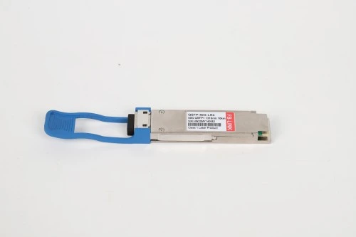
Modern transceiver high bandwidth systems operate through a three-stage process that transforms network data into transmissible optical signals. The electrical interface receives data from network switches at rates up to 425 Gbps (accounting for overhead in 400G systems), while the optical interface transmits this data over distances ranging from 70 meters to 80 kilometers depending on the module type.
Silicon photonics has emerged as the dominant platform for these devices. Intel shipped over 1.7 million silicon photonic transceivers in 2023 alone, capturing a market segment that now represents more than 20% of all datacom optical transceivers. The silicon photonic integrated circuit (PIC) market grew from $95 million in 2023 to a projected $863 million by 2029, demonstrating a 45% compound annual growth rate.
The fundamental advantage lies in integration density. Traditional transceiver designs require separate components-lasers, modulators, photodetectors-each manufactured independently and assembled manually. Silicon photonics consolidates these elements onto a single chip using existing semiconductor fabrication infrastructure, reducing production costs by up to 30% while cutting power consumption by 20% compared to discrete component architectures.
Three continuous-time linear equalizers handle signal compensation at different frequency bands. The first stage boosts high-frequency signals near the Nyquist frequency with peak gains reaching 17 dB, the second compensates for mid-frequency loss at 10 GHz to eliminate inter-symbol interference, while the third maintains constant DC gain for low-frequency stability. Variable gain amplifiers then scale the signal amplitude before saturation amplifiers prepare the signal for sampling.
Bandwidth Scaling Across Transceiver Generations
Optical transceiver bandwidth has scaled by 16× in just over a decade, moving from 100 Gbps per port in the early 2010s to 1.6 Tbps proof-of-concept modules entering field trials today. Each generational leap changes more than raw speed. Lane architecture, SerDes requirements, power efficiency, and cost economics shift together, and understanding these interdependencies determines whether a bandwidth upgrade delivers its promised return or creates new bottlenecks.
The 100G generation established the baseline. QSFP28 modules split 100 Gbps across four lanes running 25 Gbps NRZ each, with total module power consumption sitting at 3.5 watts. At an average selling price of $100–150 per unit in 2024, the effective cost works out to roughly $1.00–1.50 per Gbps. These modules pair with 25G SerDes on host switch ASICs, a mature electrical interface that tolerates substantial PCB trace loss without equalization. For enterprise campus networks and storage fabrics where per-port bandwidth requirements plateau below 100 Gbps, this generation remains the volume sweet spot-approximately 60% of global transceiver shipments in 2024 still fell within the 10–40G and 100G range.
Moving to 400G changes the engineering calculus. Two distinct electrical interfaces coexist: 8×50G PAM4 (used in QSFP-DD and OSFP modules paired with 50G SerDes ASICs like Memory Broadcom Memory Tomahawk 3/4) and the newer 4×100G PAM4 (for 100G SerDes platforms including Tomahawk 5). The optical side typically condenses further-400G-FR4 and LR4 variants use a gearbox to convert eight electrical lanes into four optical wavelengths at 100G each, reducing fiber count from eight strands to four. Module power consumption rises to 10–12 watts for standard QSFP-DD variants and 15–20 watts for coherent ZR pluggables rated for 80 km DCI spans. With 2024 ASPs of $500–700 per unit, the cost per Gbps drops to $1.25–1.75-comparable to 100G on a per-bit basis but with 4× the port capacity in an identical front-panel footprint.
The 800G generation brings a more aggressive efficiency gain. Eight lanes at 100 Gbps PAM4 deliver the full 800G aggregate through OSFP or QSFP-DD800 form factors. The critical enabler here is the 100G SerDes, which achieved production maturity in 51.2T switch ASICs during 2024. Because the 800G optical interface maps 1:1 to the electrical interface-eight optical lanes directly matching eight SerDes lanes-no internal gearbox conversion is needed for DR8 and SR8 variants. Eliminating the gearbox saves 2–3 watts per module. Total power consumption for 800G SR8 modules lands around 14–16 watts, which translates to approximately 17–20 picojoules per bit. That figure represents a 30–40% improvement over the 25–30 pJ/bit typical of 400G QSFP-DD modules, confirming the trend that bandwidth scaling through lane-speed increases consistently outperforms scaling through lane-count multiplication in energy terms.
Where the generational comparison becomes most relevant for procurement planning is the aggregate fabric cost. Consider a leaf-spine fabric connecting 512 GPU servers, each with four 400G network ports. The leaf layer requires 2,048 switch ports at 400G. Upgrading the spine to 800G halves the required port count to 1,024 while maintaining the same bisection bandwidth, which directly reduces the number of spine switches, cabling runs, and optical modules needed. At current 800G pricing (early-volume ASPs around $1,200–1,500 per unit), the cost per Gbps sits at $1.50–1.88-higher than mature 400G pricing, but the system-level savings from reduced switch count and simplified cabling typically offset the module premium by 15–25% in total fabric cost.
Looking at the 1.6T horizon, the lane architecture faces a fork. One path doubles the lane count to sixteen at 100G each (16×100G), staying within proven SerDes technology but requiring new form factors wider than current OSFP. The alternative doubles lane speed to 200G across eight lanes (8×200G), maintaining the existing OSFP-XD form factor but demanding 200G SerDes-a technology that requires next-generation 102.4T switch ASICs currently in development. Early 1.6T pluggable prototypes entering field trials in 2025 consume 20–25 watts, yielding approximately 12–16 pJ/bit. If these power targets hold through production ramp, 1.6T modules would achieve roughly half the energy-per-bit of today's 400G transceivers for data center interconnect applications.
The SerDes generation on the host switch determines which transceiver bandwidths can be deployed without electrical retiming. A 25.6T switch built on 50G SerDes natively supports 400G QSFP-DD (8×50G) but requires a retimer or gearbox to interface with 800G optics-adding latency, power, and cost that partially negate the bandwidth upgrade. The 51.2T generation with 100G SerDes natively supports both 400G (4×100G) and 800G (8×100G), making it the natural inflection point for 800G adoption. Organizations planning transceiver purchases need to verify their switch ASIC generation first; buying high-bandwidth optical modules without matching electrical infrastructure creates an expensive mismatch that no amount of signal processing can fully compensate.
Breakout configurations add another dimension to the bandwidth comparison. An 800G OSFP 2FR4 module splits into two independent 400G-FR4 streams over separate fiber pairs, allowing a single switch port to serve two distinct 400G connections. This capability proves particularly valuable during transition periods when a network runs a mix of 400G and 800G endpoints. Similarly, 400G-DR4 modules support breakout into four independent 100G links using MPO-to-LC harnesses, extending the useful deployment life of 400G-capable switch ports in environments where many connected devices still operate at 100G. These breakout modes mean the effective bandwidth utility of a transceiver purchase extends well beyond its nominal rate specification.
For AI training clusters specifically, the bandwidth requirement calculation maps directly to GPU interconnect topology. A single Nvidia DGX H200 system generates 3.6 Tbps of network traffic across its eight 400G NIC ports during all-reduce operations. Scaling to a 10,000-GPU cluster with fat-tree topology demands roughly 5,000 spine-layer switch ports at 800G-or equivalently, 2,500 ports at 1.6T-just for the GPU communication fabric, before accounting for storage and management networks. This arithmetic explains why hyperscale operators committed to 800G DR8 volumes exceeding 5 million units in 2024 and are already qualifying 1.6T prototypes: each generational bandwidth increase directly reduces the physical switch and cabling layer that represents both the largest cost and the longest lead-time item in cluster construction.
PAM4 Modulation: The Bandwidth Multiplier
Pulse Amplitude Modulation 4-level represents the technical breakthrough enabling transceiver high bandwidth performance at 400G and 800G over existing infrastructure. Where traditional NRZ (Non-Return-to-Zero) modulation uses two signal levels to transmit one bit per symbol, PAM4 employs four distinct amplitude levels-representing 00, 01, 10, or 11-to transmit two bits per symbol.
This doubles the effective data rate without requiring a proportional increase in baud rate. An 800G network runs on eight lanes at 100 Gbps (50 GBaud PAM4) rather than sixteen lanes at 50 Gbps NRZ. The math is straightforward: halving the number of required lanes cuts cabling costs, reduces switch port density requirements, and extends the usable lifespan of existing fiber installations.
The tradeoff appears in signal-to-noise ratio. PAM4's four amplitude levels compress into the same voltage swing as NRZ's two levels, reducing the spacing between levels to one-third of NRZ spacing. This creates a theoretical SNR penalty of approximately 10 dB (20 × log₁₀(1/3)), making PAM4 signals significantly more susceptible to noise, crosstalk, and dispersion.
Forward error correction compensates for this vulnerability. Modern PAM4 transceivers implement sophisticated FEC algorithms on both transmit and receive sides, encoding data before transmission and correcting errors upon reception. Testing has shown that properly designed PAM4 transceivers can compensate for up to 25 dB of channel loss while maintaining bit error rates below 10⁻¹² with three-tap feedforward equalization.
The power consumption equation remains complex. PAM4 modulation requires extensive digital signal processing for equalization and pre-compensation at both transmission ends. A 1.6 Tbps transceiver typically consumes around 30 watts, with DSP circuits accounting for more than half that power draw. Yet this still represents improvement over running double the number of NRZ lanes to achieve equivalent transceiver high bandwidth capacity.
Real-world deployment at AT&T illustrates the scale. Their 400G-based IP backbone carries 594 petabytes of domestic traffic daily, with architecture designed to scale as bandwidth demand rises. QSFP28 PAM4 DWDM transceivers now support up to 4 Tbps aggregate bandwidth over single fiber strands at distances reaching 80 kilometers, validated through field testing that confirms tolerance to dispersion and fiber nonlinear effects.
Form Factor Evolution and Port Density
The transceiver industry has converged around QSFP (Quad Small Form-Factor Pluggable) standards for transceiver high bandwidth applications, though complexity has increased with each generation. QSFP28 dominates 100G deployments with standardized 4×25 Gbps lanes, while QSFP-DD (Double Density) and OSFP (Octal Small Form-factor Pluggable) compete for 400G market share.
QSFP-DD maintains backward compatibility with QSFP28 mechanical specifications while doubling the electrical lanes to eight, enabling 400G transmission via 8×50 Gbps PAM4 signaling. OSFP provides higher power delivery capacity-up to 15 watts versus QSFP-DD's 12 watts-critical for DSP-intensive coherent modules. However, OSFP introduces its own complexity with three distinct form factors: open-top, close-top, and riding heat sink configurations.
The 800G generation fragments further. Some implementations use OSFP FIN with eight lanes at 100 Gbps per lane, while others deploy OSFP112 or QSFP112 variants. Network engineers must verify connector compatibility carefully, as certain 400G network interface cards accept only flat-top OSFP modules, rejecting FIN designs despite shared electrical specifications.
Shipment data from 2024 reveals the competitive landscape. Approximately 60% of transceiver volumes fell within the 10-40 Gbps range, serving the installed base of enterprise and telecom infrastructure. Single-mode fiber transceivers captured 61% of total shipments, preferred for long-haul telecommunications, while multimode variants held 39%, concentrated in short-reach data center applications.
The hyperscale operators are pushing boundaries faster. Google and competing cloud providers surpassed 5 million units of 800G DR8 devices during 2024, endorsing the transition to next-generation bandwidth density. First-generation 1.6T pluggable proof-of-concept modules entered field trials in late 2024, targeting commercial release by end of 2025. InnoLight planned to ship 3 million silicon photonic modules in 2024 alone, indicating the velocity of technology adoption.
Data Center Traffic Patterns and Infrastructure Demands
Global data center installed capacity grew fivefold between 2005 and 2025, reaching 114 gigawatts. Annual growth rates accelerated dramatically after 2018, with capacity installations posting double-digit percentage increases every year through 2025. The 2019 growth rate of 18.6% marked the fastest expansion, while 2025's estimated 17.7% increase ranks second-best in the measurement period.
This infrastructure buildout responds to relentless traffic growth. Data center facilities consumed 485 terawatt-hours of electricity in 2024, representing 1.7% of global electricity demand. Projections indicate consumption will nearly double to 945 TWh by 2030, driven primarily by AI model training and inference workloads.
Asia-Pacific leads regional capacity deployment with 12.2 gigawatts live in 2024, forecast to reach 26.1 GW by 2028-a 21% annual growth rate. The region consumed approximately 320 TWh of electricity for data center operations in 2024, with demand potentially hitting 780 TWh by 2030. Renewable energy sources may supply only 32% of this requirement, creating significant pressure on grid infrastructure.
Rack density metrics tell the power story more vividly. Traditional server racks consume 5-10 kilowatts per rack, but next-generation GPU clusters push requirements to 250 kW per rack. AI workloads create this density explosion: a single Nvidia DGX H100 GPU server system ships with four 400G ports, necessitating leaf-spine fabric networking at 800 Gbps port densities. This level of interconnectivity demands high-speed optical interconnect solutions that can handle the massive east-west traffic patterns characteristic of AI training clusters.
The north-south traffic pattern-data moving between servers and external networks-historically dominated data center designs. AI training reverses this. East-west traffic between servers within the data center now comprises the majority of bandwidth consumption, with training clusters requiring all-to-all connectivity patterns that stress network topologies in ways traditional web applications never did.
Meta's capital expenditure trajectory illustrates the investment scale. Their spending could reach $65 billion in 2025, up from $38-40 billion in 2024, largely allocated to AI infrastructure. Microsoft plans $80 billion in fiscal 2025, having invested $40 billion in AI data center capacity during 2024. Google budgets $75 billion, Amazon $100 billion-these figures represent the largest infrastructure buildout in modern computing history.
Coherent vs Direct Detection: Choosing the Right Technology
The modulation format decision separates into two camps based on transmission distance and capacity requirements. Direct-detect PAM4 serves short to medium distances (up to tens of kilometers) with cost-effective implementations prioritizing simplicity. Coherent modulation targets long-haul applications requiring maximum spectral efficiency over hundreds of kilometers. Organizations deploying transceiver high bandwidth infrastructure must carefully evaluate which approach matches their specific distance and capacity needs.
Coherent systems modulate both amplitude and phase of the optical signal, employing advanced formats like QPSK (Quadrature Phase Shift Keying) and QAM (Quadrature Amplitude Modulation). QAM-16 encodes 4 bits per symbol, achieving spectral efficiency that dwarfs PAM4's 2 bits per symbol. This efficiency comes at substantial cost: coherent transceivers require local oscillators, sophisticated DSP engines, and complex receiver architectures that drive power consumption to 30+ watts per module.
The application boundary sits around 80 kilometers. For data center interconnects within metro areas, 400G ZR/ZR+ coherent pluggables combined with passive Mux/DeMux filters can achieve up to 75% cost savings compared to traditional muxponder-based DWDM systems. Below 80km, IP-over-DWDM architectures using these transceivers simplify point-to-point networking dramatically, eliminating multiple layers of optical transport equipment.
For distances under 25 kilometers where DWDM wavelength selection matters but cost sensitivity dominates, 100G O-Band DWDM transceivers offer a middle path. These modules support up to 16-channel passive multiplexing with estimated cost savings around 30% compared to full open line systems, while avoiding the complexity of coherent detection.
Market segmentation data shows data centers accounted for 61% of optical transceiver revenue in 2024, growing at 14.87% CAGR-the fastest-growing application segment. Hyperscale operators increasingly procure transceivers directly rather than through intermediaries, doubling coherent-pluggable sales to approximately $600 million in 2024. Telecommunications and enterprise segments split the remaining 39% of revenue, with telecommunications providers deploying coherent modules for long-haul and regional networks.

Power Efficiency Through Co-Packaged Optics
Traditional pluggable transceivers connect to switches via faceplate-mounted cages, requiring signals to traverse 14-16 inches of printed circuit board traces and copper cabling. This lengthy electrical path introduces losses, reflections, and crosstalk that degrade signal integrity. Digital signal processors compensate for these impairments, adding latency (typically 30-50 nanoseconds) and consuming substantial power.
Co-packaged optics (CPO) eliminates this signal path. By integrating silicon photonic transceivers directly onto the same package as the switch ASIC, the electrical connection shrinks from inches to millimeters. Signal integrity improves dramatically, allowing the elimination of the external DSP entirely. Early implementations demonstrate power consumption reductions of 3.5× compared to pluggable transceivers at equivalent data rates.
Nvidia's announcement at GTC 2025 illustrated the approach. Their Quantum and Spectrum switch ICs now integrate silicon photonics directly on-package, achieving the 3.5× power reduction while simultaneously improving network resiliency and reducing latency. For AI data centers where a 1.6 Tbps pluggable transceiver might consume 30 watts (with DSP taking 15+ watts), co-packaged alternatives could operate at 8-10 watts.
The reliability equation also shifts. Pluggable transceivers depend on mechanical connectors, contact pressure, and thermal management of discrete components-all potential failure points requiring manual troubleshooting that can take hours. CPO's integrated design features fewer components and simpler thermal management, potentially reducing failure rates by order of magnitude.
Deployment speed improves measurably. Transceiver-based systems require technicians to manually seat dozens or hundreds of modules, verify connections, and troubleshoot any DOA (dead on arrival) units. CPO switches arrive with optics pre-integrated, enabling what Nvidia describes as "unbox and install" deployment 1.3× faster than conventional systems.
The technology remains in early adoption. Manufacturing co-packaged optics requires coordination between switch designers, optical engineers, and semiconductor foundries that traditional module vendors haven't needed. Thermal management becomes more challenging when optical and electronic components share a single package operating at different temperature optima. The industry estimates widespread CPO deployment won't reach scale until 2026-2027 as these manufacturing challenges resolve.
Wavelength Division Multiplexing for Maximum Fiber Utilization
Dense Wavelength Division Multiplexing (DWDM) multiplies effective fiber capacity by transmitting multiple independent data streams on different optical wavelengths through a single strand. Modern DWDM systems support 96 wavelengths in the C-band spectrum (1530-1565 nm), each potentially carrying 100G, 400G, or 800G of traffic. When combined with transceiver high bandwidth modules, DWDM enables aggregate capacities exceeding 38 terabits per second over a single fiber pair.
The wavelength grid follows ITU standards, typically spacing channels at 50 GHz (approximately 0.4 nm) or 100 GHz (approximately 0.8 nm) intervals. Passive optical components-arrayed waveguide gratings or thin-film filters-combine (multiplex) these wavelengths at the transmit side and separate (demultiplex) them at the receive end, requiring no active power for the wavelength selection itself. For detailed guidance on channel allocation strategies, see this DWDM wavelength planning guide for C-band and L-band.
QSFP28 100G DCO (Digitally Coherent Optics) transceivers exemplify the technology's evolution. These modules achieve 80-kilometer transmission without amplification while maintaining backward compatibility with existing QSFP28 ports. By incorporating tunable lasers, field technicians can adjust wavelengths to match specific DWDM channel plans, providing flexibility that fixed-wavelength modules cannot.
The aggregate capacity calculation becomes compelling. A 96-channel DWDM system with 100G per wavelength delivers 9.6 Tbps over a single fiber pair. Upgrading to 400G per wavelength pushes capacity to 38.4 Tbps. Given that installing new fiber-particularly in dense urban environments or submarine cables-costs millions of dollars per route mile, DWDM represents dramatic capital efficiency.
Real-world implementations vary by distance and application. Data center interconnects within a campus (< 2km) often use Coarse WDM (CWDM) with wider channel spacing and fewer wavelengths, reducing component costs. Metro networks (2-80km) deploy DWDM over passive infrastructure. Long-haul networks (> 80km) add optical amplifiers every 60-100 kilometers, reconfigurable optical add-drop multiplexers, and sophisticated network management systems.
The tuning system in modern transceivers allows wavelength adjustment in the field, adapting to changing network requirements without physical module replacement. Operators can shift capacity between routes by simply retuning wavelengths and updating routing tables, providing operational agility that fixed-wavelength systems cannot match.
Market Dynamics and Regional Growth Patterns
North America captured 39% of the data center networking market in 2024, driven by widespread hybrid and multi-cloud deployments across enterprise, government, and education sectors. The U.S. market specifically is projected to grow at 16% CAGR through 2033, fueled by expansion of AI research hubs and high-performance computing clusters in healthcare, defense, and academia.
China's position in Asia-Pacific deserves specific attention. The country held substantial market share in 2024 through its focus on technological self-sufficiency and domestic cloud ecosystem expansion. National policies including the New Infrastructure initiative and digital industrialization drive Chinese cloud providers to invest heavily in proprietary data center networking systems. The country accounts for approximately 49% of overall Asia-Pacific data center investments.
Europe's FLAP-D markets-Frankfurt, London, Amsterdam, Paris, Dublin-accounted for nearly 50% of new European capacity in 2025, though each faces distinct constraints. Frankfurt maintains the lowest vacancy rate at 6%, with power availability limiting development. Amsterdam's connectivity hub status attracts demand, but stringent regulations and power limits slow construction. London's supply shortage persists despite strong demand, particularly from hyperscalers in the western corridor.
The optical transceiver market shows regional variations in revenue concentration. Asia-Pacific leads with 39% of global shipments in 2024, North America follows at 35%, Europe captures 25%, while Middle East and Africa account for 1-5%. Growth rates diverge significantly: Asia-Pacific posts the fastest expansion driven by 5G rollouts and cloud infrastructure, while mature markets in North America and Europe show steadier but substantial growth.
Pricing trends reflect manufacturing scale economies. Average selling prices for 400G transceivers declined from $800-1,200 per unit in 2022 to $500-700 by 2024 as production volumes increased and silicon photonics manufacturing matured. Similar patterns appeared in 100G pricing, which compressed from $200-300 to $100-150 over the same period. However, bleeding-edge 800G and 1.6T modules maintain premium pricing above $2,000 per unit during early commercial release.
Performance Benchmarking and Real-World Metrics
Transmission distance specifications vary dramatically by transceiver type and fiber quality. Short-reach modules using multimode fiber (MMF) cover 70-150 meters at 100G, suitable for connections within a single data center row or between adjacent buildings. Single-mode fiber (SMF) extends reach: 100G transceivers reliably operate over 10 kilometers for intra-campus links, while extended-reach variants push to 40 kilometers for metro applications.
Error correction overhead consumes a measurable percentage of raw bandwidth. A "400G" Ethernet link actually operates at 425 Gbps to accommodate RS-544 FEC encoding, which adds one parity bit for every eight data bits. This 12.5% overhead prevents bit errors from corrupting data but reduces net application throughput to the nominal 400G specification.
Latency measurements separate by component. The optical flight time over fiber adds approximately 5 microseconds per kilometer-negligible for most applications but relevant in high-frequency trading where microseconds matter. Electronic processing latency varies: simple direct-detect systems add 5-10 nanoseconds, while DSP-equipped transceivers introduce 30-50 nanoseconds. Co-packaged optics minimizes this to under 10 nanoseconds by eliminating the DSP stage entirely.
Power per bit represents the critical efficiency metric. Modern 400G QSFP-DD modules consume 10-12 watts, equating to approximately 25-30 picojoules per bit. Legacy 100G QSFP28 modules use 3.5-4.5 watts, or 35-45 picojoules per bit-slightly worse efficiency due to the unfavorable scaling of fixed power consumption components. Coherent 400G ZR modules push power to 15-20 watts given their sophisticated DSP requirements. Monitoring these parameters in real time requires digital diagnostic monitoring (DDM) capabilities built into modern transceiver modules.
Temperature tolerance defines deployment flexibility. Commercial-grade transceivers operate from 0-70°C, suitable for climate-controlled data centers. Industrial variants extend to -40°C to +85°C for outdoor installations, telecommunications equipment, and edge computing locations lacking environmental control. This wider range requires different laser designs and packaging approaches that increase manufacturing cost.
Emerging Technologies and Future Roadmap
Linear Pluggable Optics (LPO) represents a recent architecture innovation that shifts DSP functions from the transceiver into the switch ASIC itself. By eliminating the module-internal DSP, LPO transceivers reduce power consumption and cost while maintaining compatibility with existing form factors. Industry estimates suggest LPO could reduce 800G module costs by 30-40% compared to conventional DSP-equipped designs, making transceiver high bandwidth solutions more accessible for a broader range of data center deployments.
The technology faces standardization challenges. Different switch vendors implement DSP capabilities differently, and ensuring cross-vendor compatibility requires industry agreement on electrical specifications, link training procedures, and performance parameters that remain under development in IEEE and OIF working groups.
Research into PAM6 and PAM8 modulation continues, though noise margin constraints may limit practical deployment. PAM6 uses six amplitude levels per symbol (representing 2.6 bits), while PAM8 employs eight levels (3 bits per symbol). The signal-to-noise requirements become increasingly stringent with each additional level, potentially limiting these formats to very short reach applications or requiring exotic FEC overhead that negates the capacity benefit.
3.2 Tbps pluggable transceivers entered field trials in late 2024, targeting 2026 production deployment. These devices employ either 16 lanes at 200 Gbps per lane or 8 lanes at 400 Gbps per lane, both representing substantial advances beyond current 100 Gbps-per-lane technology. The 200G SerDes would require next-generation network processors with 102.4 Tbps ASIC capacity-devices that are themselves in development cycles aligned with the optical module roadmap.
Quantum computing and optical computing applications represent longer-term opportunities for photonic integration. While traditional transceivers convert data between electrical and optical domains, future architectures might maintain signals in the optical domain throughout processing stages. Silicon photonics provides a platform for integrating optical waveguides, modulators, and detectors with quantum photon sources and single-photon detectors, enabling chip-scale quantum information processing.
The sustainability dimension grows more prominent. Data centers already account for 1.7% of global electricity consumption, and this percentage will increase unless efficiency improves dramatically. Industry commitments like Europe's Climate Neutral Data Centre Pact mandate 100% renewable energy by 2030, creating pressure for continued power reduction in every component. Transceivers consuming 3.5× less power through co-packaging approaches represent meaningful contributions toward these targets. For organizations planning upgrades in this evolving landscape, optical capacity planning to future-proof fiber networks becomes an essential strategic exercise.
Frequently Asked Questions
What determines the maximum bandwidth a transceiver can handle?
The maximum bandwidth depends on three primary factors: the modulation format (PAM4 doubles capacity over NRZ), the number of parallel lanes (8-lane designs support higher aggregate rates than 4-lane), and the speed per lane (current technology reaches 100 Gbps per lane, with 200 Gbps under development). A 400G transceiver typically uses 8 lanes at 50 Gbps PAM4, while 800G employs 8 lanes at 100 Gbps. Physical constraints like laser bandwidth, photodetector response time, and fiber dispersion ultimately limit how fast each lane can operate.
How does transceiver bandwidth differ from network throughput?
Transceiver bandwidth refers to the raw signal rate-the physical layer capacity. Network throughput accounts for protocol overhead, error correction, and actual data payload. A 400G transceiver operates at 425 Gbps raw rate to accommodate forward error correction overhead, delivering approximately 400 Gbps after FEC decoding. Additional overhead from Ethernet framing, TCP/IP headers, and application protocols further reduces effective throughput. In practice, applications might see 370-390 Gbps of usable bandwidth from a "400G" connection.
Can older data centers upgrade to high-bandwidth transceivers without replacing fiber?
In most cases, yes. PAM4-based 400G and 800G transceivers were specifically designed to operate over existing OM3/OM4 multimode fiber for short distances (70-150 meters) and standard single-mode fiber for longer links. This backward compatibility makes transceiver high bandwidth upgrades economically feasible for organizations with established fiber infrastructure. The key constraint is fiber quality-older fiber may have accumulated contamination, micro-bending losses, or splice degradation that limits maximum achievable distance. A comprehensive fiber characterization (insertion loss, return loss, dispersion measurements) determines upgrade viability. Metro distances often work up to 80 kilometers without fiber replacement, though amplification might be needed.
What causes transceivers to fail in high-bandwidth applications?
Thermal stress ranks as the leading failure mechanism. High-speed transceivers generate substantial heat (10-30 watts) in a small form factor, and inadequate cooling causes components to exceed specified operating temperatures, degrading lasers and electronics. Connector contamination creates optical signal loss-a single dust particle in an optical connector can block 50%+ of the light. Power supply quality matters: voltage ripple or transients can damage sensitive circuits. Finally, firmware bugs or compatibility issues between transceivers and host equipment cause link failures that appear as physical layer problems but actually stem from software.
Which transceiver bandwidth tier offers the lowest cost per gigabit for new deployments?
As of 2024 pricing, mature 400G QSFP-DD transceivers offer the most favorable per-gigabit economics at $1.25–1.75 per Gbps, compared to $1.00–1.50 for 100G QSFP28 and $1.50–1.88 for early-volume 800G modules. However, per-gigabit module cost alone does not capture the full picture. Fabric-level analysis must account for switch port count, cabling density, power distribution, and cooling infrastructure. In leaf-spine designs serving 512 or more endpoints, 800G spine links typically reduce total fabric cost by 15–25% despite higher per-module pricing, because they halve the required spine switch count and associated cabling. The crossover point where 800G becomes more cost-effective than 400G depends on fabric scale-generally above 256 ports in the spine layer.
The infrastructure supporting global digital services rests on transceiver high bandwidth technology processing hundreds of terabits per second of data center traffic. As AI workloads drive power density to 250 kilowatts per rack and rack counts scale to support exabyte-scale data sets, optical interconnect technology advances from incremental improvement to fundamental necessity. The transition from 100G to 400G to 800G transceivers represents more than bandwidth multiplication-it embodies the architectural shift enabling the next generation of computing.
Key Takeaways
High-bandwidth transceivers achieve 100 Gbps to 1.6 Tbps per port using PAM4 modulation that doubles capacity by transmitting 2 bits per symbol rather than traditional 1 bit
Silicon photonics integration reduces transceiver production costs by 30% and power consumption by 20% compared to discrete component designs, with the market growing at 45% CAGR
Data center capacity grew fivefold from 2005 to 2025, reaching 114 gigawatts, driven by AI workloads that account for 40% of demand growth through 2030
Co-packaged optics eliminate external DSPs and reduce signal paths from 14 inches to millimeters, achieving 3.5× power reduction compared to pluggable transceivers
DWDM systems multiply fiber capacity by transmitting 96 wavelengths per strand, delivering up to 38.4 Tbps with 400G per wavelength
Data Sources
Fortune Business Insights - Optical Transceiver Market Analysis 2024-2032
International Energy Agency - Data Center Capacity Report 2025
McKinsey & Company - Data Center Demand Forecasts 2030
IDTechEx - Silicon Photonics Market Research 2024-2034
MarketsandMarkets - Optical Transceiver Market Report 2024-2029
Yole Intelligence - Silicon Photonics Industry Report 2024
NVIDIA - GTC 2025 Co-Packaged Optics Announcement
community.fs.com - High-Speed Optical Transceiver Technical Documentation
Juniper Networks - 400G Transceiver Technical Guide
IEEE 802.3 - Ethernet Standards Documentation